- HubPages»
- Technology»
- Computers & Software»
- Computer Hardware
How to understand Memory Timings

Introduction
This Hub is intended to go deeper into the topic "memory timings". In my previous Hub I talked about how memory works and what the differences are between DDR, DDR2 and DDR3. Memory Timings is a very interesting topic which deserves to be in a separate Hub (this one). It’s a piece of interest of mine for many years. It’s pretty technical and also you have to be interested and have a bit of pc skill to understand the following material. I hope it will help you like it helped me!
Basics
Quick view on timings and a recap
This is a quick recap on some things previously discussed in Hub called: Everything you need to know about system memory. DDR, DDR2 and DDR3 are memory that is classified by there maximum MHz speed primarily. I am not going deep into stuff already discussed but I’ll quickly mention some terms to fresh up the memory. Also a new term will be introduced called “memory timings” which are numbers like 3-5-5-8 or 5-5-5-18 or 7-7-7-20 or 9-9-9-24. The lower those numbers are the better it is for your performance. I’ll go into those numbers what they are exactly and what they mean also performance wise.
DDR, DDR2 and DDR 3 use a classification system by DDRxxx/PCyyyy. This can be found in my other Hub called:Everything you need to know about system memory. The “xxx” represent the maximum “clock rate speed” like DDR400 operates at 200 MHz, DDR2-800 operates at 400 MHz and DDR3-1333 at the real speed of 666 MHz.
The “yyy” represents the “maximum transfer rate” that’s presented in MB/s which the memory can reach at the max. So when memory can reach 3200 MB/s max it’s memory module is labelled PC3200. PC2-6400 is called DDR2-800 because it transfers 6400 MB/s max. And DDR3-1333 has a max of 10664 MB/s so it’s called PC3-10600. The 2 or 3 indicate the generation of memory and if we are discussing DDR2 or DDR3.
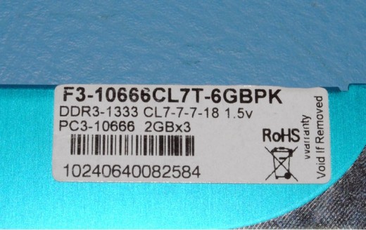
DDRxxx is used to classify the standard for memory chips and PCyyyy is used to classify the standard for memory modules. On the right picture you see PC3-10666/10600 memory module. It’s a DDR3-1333 memory module chip. There you see the timings (7-7-7-18 and it’s voltage (1.5V).
Calculation for “maximum transfer rate” = Clock Rate Speed x amount of bits / 8
Because memory modules always transfer 64 bits each time and divide that with 8 makes 8. So we can make the formula simpler:
Calculation for “maximum transfer rate”= Clock Rate Speed x 8
A common misjudgement is made when you install your memory modules in a motherboard that has a lower memory bus speed and therefore a lower clock rate. I’ll make an example with a pair of DDR3-2133 (PC3-17000) memory modules. These modules have a label for DDR3-2133 but they won’t run at 2133 MHz automatically in your pc. DDR3-2133 is the maximum clock rate speed the memory supports but not the clock rate speed it will actually run at always. In a regular pc with DDR3 support the memory will likely run at 1333 MHz (DDR3-1333) and this is the maximum DDR3 standard. So the difference is if it runs on 1333 MHz instead of 2133 MHz you will get 10664 MB/s compared to 17000 MB/s. DDR3-1333 (1333 mhz) = 8 x 1333 = 10664 (MB/s) and DDR3-2133 (2133 MHz) = 8 x 2133 = 17000 (MB/s). This doesn’t mean you will always get that amount of MB/s but it’s the max you can possible have. And you rather have a larger maximum limit then a smaller limit of MB/s.
The reason for some people to buy these memory modules is because they like to overclock. Because the manufacturer gives you a guarantee that these fast memory modules can really run at 2133 MHz. This is very useful when you want to raise the memory bus clock speed to a speed of 1066 MHz, so you can get the most performance out of your pc. If you’re not going to overclock your pc it’s pretty useless and waste of money if you buy memory modules that have a higher speed then the speed your motherboard supports.
These are the most average things I’ll tell in this Hub about memory. Like I said an advanced explanation you can find in my other Hub: Everything you need to know about system memory. So now comes the part where we get into a advanced characteristics like timings/latency.
Memory Timings
Due to timings, 2 different memory modules can have different levels of performance but with a maximum transfer rate that is equal. The reason is the following explanation.
The time memory chips are delayed doing things is measured in time called timings. The most important parameter called CAS (latency, CL or “access time”), which shows the amount of clock cycles the memory module delays when it returns its data that a processor requests. Memory modules that have a CAS of 9 have a delay of 9 “clock cycles” for a request of data to be delivered. Memory modules that have a CAS of 7 however have a delay of 7 “clock cycles” for a request of data to be delivered. When you have a memory module at the same speed the last one with CAS 7 will be faster, because it has less delay and will supply data quicker then the memory module with CAS 9 (2 clock cycles faster).
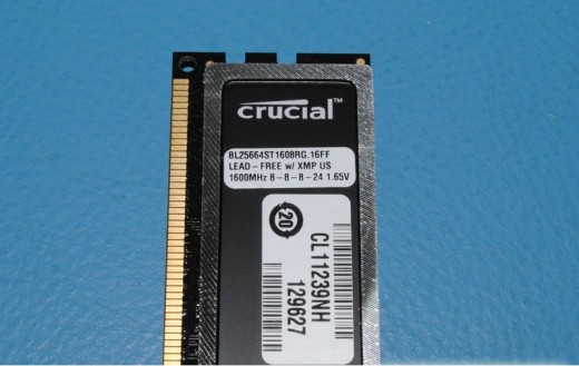
Cas is not the only number you can see on the picture right. You see more numbers that indicate other operations and the clock cycles it takes to perform them. The lower the number means the faster the memory. The memory module on the right picture is a DDR3-1600 (PC3-12800) and shows the timings: 8-8-8-24.
These numbers that represent the timings are indicated as follows: CL – tRCD- tRP-tRAS-CMD. The memory is organized internally as a matrix so keep this in mind to understand the timings. This data is stored in an intersection comprised of lines and columns.
- CL (Cas): Cas Latency. The time it takes when a command is being sent to memory and the reply to it. So this is the time between the CPU asking for data from the memory and then the return of it.
- tRCD: RAS to CAS Delay. This is the time between the activation of the line (RAS) and the column (CAS). This is where data gets stored in the matrix.
- tRP: RAS Precharge. This is the time between when access is disabled to a line of data and the start of access to another.
- tRAS: Active to Precharge Delay. This is the waiting time until the memory can be accessed again.
- CMD: Command Rate. This is the time between the activation of the memory chip and the first command that could be send. 2 value’s are usually used T1 (1 clock cycle) or T2 (2 clock cycles). This value is sometimes not announced!
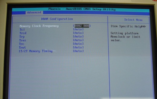
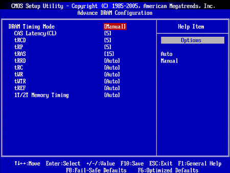
When you configure your pc there are usually 2 options to configure the memory and use the standard timings. You can either use “Auto” or “Manual” in the motherboard setup, and with the last you can use lower memory timings to increase system performance. The motherboard setup is the BIOS (Basis Input Output System and can be reached by pressing “delete” when the pc boots up. Keep in mind not all motherboards allow you to alter the memory timings. Also not all of them will allow you to run your memory at very low timings and therefore configure the memory modules to run at higher timings due to this.
If you want to overclock your memory, you may need to increase the timings of your memory so that your pc will run more stable. Interesting is because of the increase of timings the memory will achieve slower performance, even though of the higher clock rate speed but due to the higher latency.
This is also a reason people who want to overclock there memory and why this is another advantage of those special expensive memory modules. Those modules not only guarantee the memory will run at the labelled clock rate speed but also guarantee the labelled timings on that labelled MHz speed.
To give an example, you could achieve 1600 MHz (800 MHz x 2) with DDR3-1333 (PC3-10600) memory modules but it’s very likely you have to raise the memory timings. But with DDR3-1600 (PC3-12800) modules the manufacturer will guarantee you can achieve 1600 MHz keeping the timings that are labelled on the memory module.
Now I’ll go into all the memory timings and it’s parameters in detail.
CL-tRCD-tRP-tRAS-CMD (5-5-5-15-2)
(CL) CAS Latency
This is already mentioned but “CAS Latency” is the best known parameter for memory. It shows how many “clock cycles” the memory will delay to return the data that is requested. CL 7 (CAS 7) has a delay of 7 clock cycles where CL 9 (CAS 9) will have a delay of 9 clock cycles to perform the same operations. So if you have 2 memory modules running at the same clock memory speed the memory module with the lowest CAS is faster.
Keep in mind that the clock rate speed here is the real clock rate speed the memory runs on which is half the rated clock rate speed. This because DDR, DDR2 and DDR3 produces 2 data chunks each clock cycle. This is also rated with there double rated clock speed.
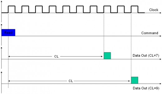
On the picture right when you click on it you see how CL works. You see the 2 examples of a memory module with CAS 7 and one with CAS 9. The blue command is the “read” command.
CL 7 has an improvement of 22.2% improvement on memory latency compared to CL9 memory in the case they run on the same speed (MHz).
To calculate the memory delay until the point it will start delivering is: T = 1 / f
A DDR3-1333 memory module at 1333 MHz (666 MHz) runs at a clock cycle of 1.5 ns (ns=nanosecond, 1 ns=0.000000001 s). You have to use the real clock rate speed which is half of the clock rate speed that is labelled on the memory. For DDR3-1333 memory the total delay with CAS 7 would make 10.5 ns and 13.5 ns if the memory had CAS 9.
DDR, DDR2 and DDR3 have an implemented burst mode which is used for data storage. This data can exit at the next addresses at each clock cycle. So the first data would delay the CL clock cycles when it exits the memory and the next piece of data would be send just after the prior data that just was released from the memory. So there will be no waiting on another CL cycle.
(tRCD) RAS to CAS Delay
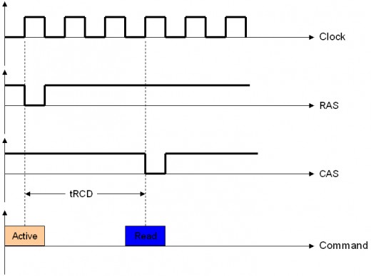
Memory chips are internal organized as a matrix. Every row and column in this intersection has a little capacitor that can be charged with the storage of a “0” or “1” (data). This process when stored data is accessed inside of a memory chip is done by the activation of the row first, and the column afterwards where data is located. The activation is accomplished with the use of 2 control signals that are called RAS (Row Address Strobe) and CAS (Column Adress Strobe). The data will be read quicker if those 2 signals will have less time between them. And tRCD (RAS to CAS) measures this time and the picture on the right shows this with a tRCD of 3.
tRCD is also the amount of clock cycles between an “Active” command and “read/write” command.
Also tRCD works with the real clock rate speed (half the labeled MHz speed). Memory will be faster when this parameter is a low as possible (the lower the better) because it will begin reading and/or writing data earlier.
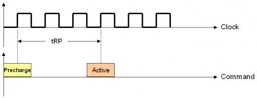
tRP (RAS Precharge)
The data from the memory that is gathered needs to be Precharged so it can close the memory row that was in use so it can activate a new row. The time between a precharge command and the following Active command that’s been issued is called tRP (RAS Precharge). As stated in the previous section an Active command begins a read or write cycle. On the right side you see a picture with a tRP of 3.
Like all the other parameters tRP also works with a memory real clock rate speed (half the labelled clock speed). The Active command will be given earlier when this parameter has a low value so the memory will be faster. Again the lower the better!
So adding up all the timings I’ve discussed, the time between producing a Precharge command and getting the actual data will be: tRP + tRCD + CL.
Other Parameters
There are 2 other paramaters called tRAS (Active to Precharge Delay and Command Rate (CMD). Also these timings work with the real clock rate speed of the memory and again the lower the timing to faster your memory will be.
- tRAS (Active to Precharge Delay): A precharge command can’t be given after an Active command only until tRAS has finished. This parameter will limit the memory when it starts reading/writing in a different row.
- Command Rate (CMD): The time for the memory chip being activated (through the Chip Select (CS) pin) and any other command can be send to the memory. This timing has the letter “T” with it. 1T or 2T is available which means 1 clock cycle or 2 clock cycles.


