- HubPages»
- Technology»
- Computers & Software»
- Computer Hardware
The Progression of Microprocessors - Part Two
Microprocessors the Personal Computer Years
March 16, 2011
This is the second in a series of articles about microprocessors and how they changed the world.
The first, The Progression of Microprocessors - Part One, dealt with the early processors made by Intel and Motorola. These early processors were used primarily in kit-computers by hobbyists interested in building their own computers far in advance of anything available in a store. As such they were home built with components supplied either in kit form or by companies devoted to the hobbyist interests.
This article deals with the processors that made it into "off-the-shelf" products such as the Tandy-Radio Shack (TRS) 80, Commodore PET, Apple II, and IBM 5150 (PC).
As before this article will be heavily Intel based, but Motorola, National Semiconductor and Advanced Micro Devices will also be covered.


Intel 8086
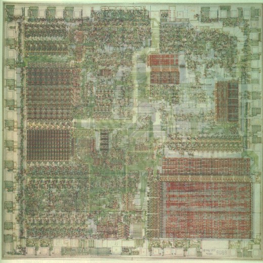
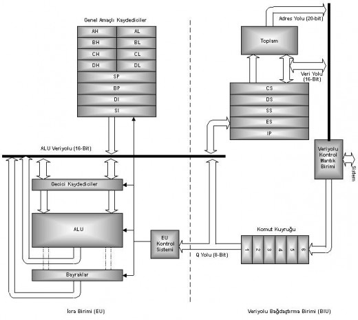
The Intel 8086 was a leap forward in microprocessor design. Where the 8080 ran at up to one MegaHertz, the 8086 ran at five to ten MegaHertz. It had twenty-nine thousand (29,000) transistors, could accept sixteen bits of information at a time, and recognized almost double the number of instructions as the 8080. It also used a new Metal Oxide Semiconductor transistor called the H MOS.
Like the 8080 before it, the 8086 could access up to one MegaByte of memory.
What made this chip different, beside the number of transistors, was the way the transistors were formed. The transistors on the 8080 required five (5V) holding voltage and twelve (12V) switching voltage. This was primarily due to the types of transistors that made up the core.
With the 8086 a new method for transistor construction was implemented called HMOS which stood for High density, short channel MOS. In essence the transistors were redesigned to lower their power requirements making the 8086 a five volt only device.A side benefit was a drastic increase in switching speed. The HMOS transistors switched four times faster than the MOSFET transistors on the 8080.
HMOS takes up less space per transistor as well which meant the chip could be more densely packed with them in the same amount of space as those in the 8080. Other benefits were faster switching and lower power requirements. The process was eventually licensed to Motorola for the 68000 chip.
The 8086 found its way into a wide variety of computers including the IBM PC, the IBM DisplayWriter (a dedicated word processor), the Wang Professional computer, the Compaq Deskpro (the first competitor to the IBM 5150 PC), the IBM PS/2, the Tandy 1000, the Amstrad PC-1512 and NASA.


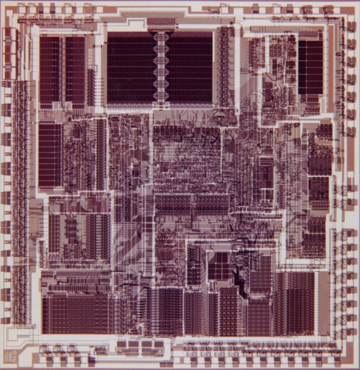
Motorola 68000
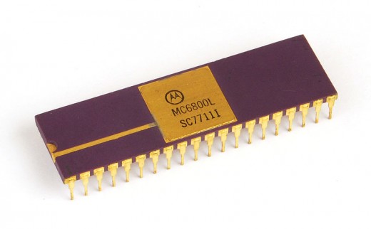
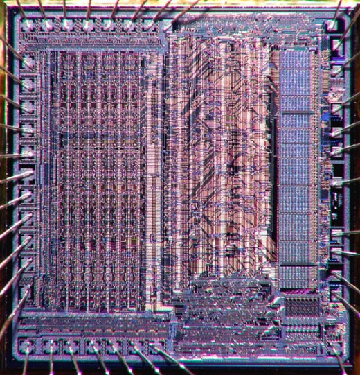
This chip was a direct descendent to the Motorola 6800. For some reason Motorola simply added another zero to the number of the chip, unlike Intel, which used a number progression to name its chips.Though 6800 and 68000 seem similar in name the next chip in Motorola's progression was also quite an advance.
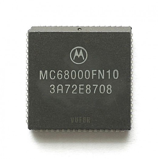
Where the 6800 had four (4,000) thousand transistors the 68000 had forty (40,000) thousand. Unlike the 6800 and 8086, the 68000 could accept data on a thirty-two (32) bit bus and access up to sixteen MegaBytes of RAM. It was also faster than its competitors at sixteen (16 MHz) MegaHertz to the 8086 top speed of eight (8MHz) MegaHertz.
As was Motorola's habit, the 68000 could be ordered with a wealth of documentation making it an easy processor to incorporate into a computer design.
The Motorola 68000 found its way into the Apple Lisa 2, Apple Macintosh 128, Atari 520ST, & 1040ST, Tandy Radio-Shack TRS-80, and the Commodore Amiga 500 and 1000. As the product matured it found its way into dedicated printers. It was the heart and soul of the Hewlett Packard LaserJet and Apple's LaserWriter.
It was also at the core of dedicated arcade games such as Atari's Food Fight and home gaming systems such as Sega's Genesis console and Atari Jaguar.
Later still a derivative of the 68000, called the Dragonball, found its way into the Palm Personal Digital Assistant (PDA) and the Handspring Visor.
The 68000 is arguably one of the most successful microprocessors ever made.
Intel 80186 & 80268
80186
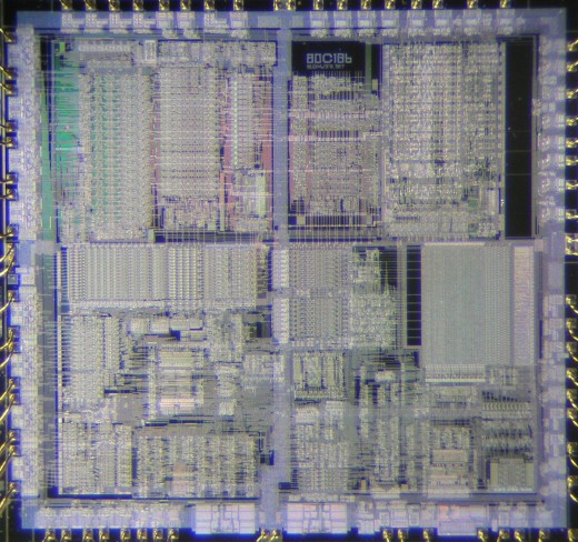
Introduced in 1982 the Intel 80186 was another leap forward in microprocessor design. Though memory addressing was still limited to one MegaByte the chip could access up to sixteen MegaBytes through software manipulation. It sported over one hundred thousand transistors and used an older technology (N-MOS) for transistor design. Though the 80186 was primary used as a dedicated processor in embedded design, in other words, as a processor for a purpose built computer, it did find its way into some personal computer offerings. This included the Wang Office Assistant, Siemens PC-D, and the Tandy 2000 desktop. However, the 80286 (below) changed the personal computer landscape.
80286
The 80286 was also introduced in 1982 with one hundred thirty-four (134.000) thousand transistors and typically ran at a clock speed of six to twelve (6~12MHz) MegaHertz. The 80286 was completely backward compatible with the 8086 processor so any computer using this processor could also run software designed for the 8086.
The 80286 was odd in that it could directly access up to one MegaByte of data in RAM, but also access up to sixteen (16MB) in protected mode. Unfortunately, this meant a special operating system that could distinguish between the protected memory and "live" memory. This lead Bill Gates, of Microsoft, to call it the "brain-dead" computer chip.
Even though the clock speed was roughly double its predecessors (the 8086), the internal design of the chip insured that it would process instructions designed for the 8086 twice as fast even running at the 8086s native clock speed. In other words the 80286 was at least four times faster than its older sibling.
This was the chip IBM chose for its next line of Personal Computers, the IBM PC/AT 5170 and a number of follow-on models. It was also the chip chosen by every clone manufacturer in the United States including Compaq.
Microsoft wrote Windows 3.0 for this particular chip, but did not know about the "protected mode" memory in time to incorporate that into its operating system. This was addressed in Windows 3.1, but by then the 80386 did away with protected memory.


Intel 80386
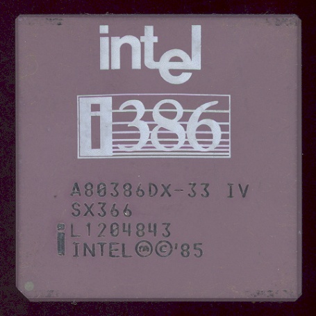
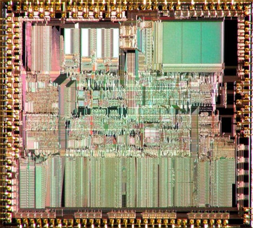
Introduced in 1985, the Intel 80386 was the first processor by that company to incorporate a thirty-two (32) bit bus for both data and addressing. It could also directly address up to four GigaBytes of memory (an astounding figure at the time) directly with no protected mode shenanigans required. This meant it was a true multi-tasking computer (the first for Intel) which would allow computer users to run a number of programs at the same time.
It had two hundred seventy five (275,000) thousand transistors in it and ran at a clock speed of sixteen (16MHz) to thirty-three (33MHz) MegaHertz. This was the chip that finally brought the personal computer into the mainstream.
Of course it was backward compatible with the 80286 and the 8080 capable of running almost all the programs written for those two earlier processors.
The 80386 appeared in the IBM Personal System 2, the Compaq Prolinea, Hewlett Pakcard Vectra and just about every other knock-off clone you can imagine.
Of all the chips mentioned in this series the 80386 had possibly the longest production life ever. It was introduced in 1985 and production on the chip was finally ended in 2007. That's a run of over twenty years. Remarkable for chip designed so long ago.
80386 Variants
Intel also wanted a slightly cheaper chip in its lineup so it also built and marketed a chip with a sixteen (16) bit bus, while the internals remained (32) thirty-two bit. This particular chip was given the designation SX after the number making it the 80368SX.
Intel automatically added a level of confusion with this newer chip and had to start adding the letter designation DX to the original 803886 so customers could tell the difference.
Intel also started making a variant just for portable computing devices called the 80386SL. Power management was a key feature of this particular processor with power down modes. The odd thing about this particular chip was that though it was essentially the same chip as the 80386 it had four times as many transistors; all devoted, I assume, to power management.


Intel 80486 & 80487
In 1989 Intel again increased processing power and capacity with the 80486. This processor ran at sixteen (16MHz) to one hundred (100MHz) MegaHertz and had an astounding one point two million (1.2M) transistors. As with the 80386, Intel had two major designs. One for desktop computers and another for portables.
The "desktop" chip was designated the 80486DX and the portable chip the 80486SX. Oddly the SX had a reduced number of transistors at just under one million where the 80386SX had four times the transistors of the 80386DX.
Unlike the 80387, 8087, and other chips marketed as Math Co-Processors the 80487 was really a CPU designed to replace and simultaneously disable the 80486SX. This, in essence, was a plug-in upgrade to the processing power of any computer equipped to run the 80486SX once the 80487DX was installed.
Intel also started incorporating the Floating Point Unit (formerly a separate chip) into the processor. They also optimized the instruction set. This set the stage for RISC (Reduced Instruction Set Computers) that followed in later years.
The 80486 was quite literally used in every IBM PC and clone imaginable.
After this Intel started naming & numbering their chips and the Pentium (8050x) followed.


Intel Pentium (80500)
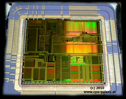
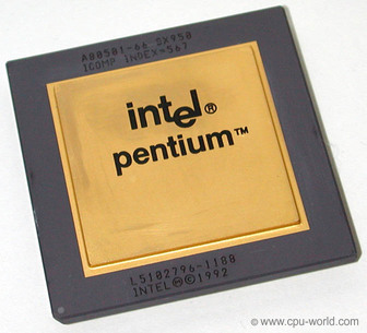
In 1993 Intel dropped the number only designation on its chips and began marketing the Pentium processor. Internally the chip still had a number; it was 80501). This processor had three point one million (3.1M) transistors. It ran at sixty to sixty six MegaHertz and was a full sixty-four bit processor with a thirty-two bit external bus.
Like the 80486 before it the Pentium had an integrated Floating Point Unit processor built in.
Rumor is that Intel switched to a name designation because number only designations could not be trademarked.
The Pentium is still in use today and Intel made (makes) a number of classes of Pentium processors with ever increasing numbers of transistors and clock speeds. In fact the Pentium III broke the GigaHertz clock barrier at 1.4 GigaHertz.
A Pentium based chip was also designed exclusively for hand-held devices, but I'll be covering chips that fall into that category in Part III.
See the table below for some of the most popular Pentium processors by transistor count and clock speed.
Pentium Classes
Pentium Name
| Clock Speed
| Transistors
|
|---|---|---|
Pentium I
| 60~66MHz
| 3,100,000
|
Pentium II
| 233~450MHz
| 7,500,000
|
Pentium III
| 450MHz ~ 1.4GHz
| 9,500,000
|
Pentium IV
| 1.3 ~ 3.8GHz
| 42,000,000
|
Wrapping Up
Though the Pentium processor family also spawned a number of processors designed specifically for handheld devices (Personal Digital Assistants and SmartPhones) I'm going to be covering those in Part III.
Stay tuned!
Disclaimer
The author was not compensated in any way, monetarily, with discounts, or freebies by any of the companies mentioned.
Though the author does make a small profit for the word count of this article none of that comes directly from the manufacturers mentioned. The author also stands to make a small profit from advertising attached to this article.
The author has no control over either the advertising or the contents of those ads.

